Search This Blog

Showing posts with label Materials Sciences Division. Show all posts

Monday, August 26, 2013

Size Matters as Nanocrystals Go Through Phases


Paychex Payroll Services: Sign up Today!


Berkeley Lab Researchers at the Molecular Foundry Reveal Fundamental Size-Dependence of Metal Nanocrystals Undergoing Phase Transitions

AUGUST 26, 2013
Lynn Yarris (510) 486-5375  lcyarris@lbl.gov
 3 


Palladium nanocubes interacting with hydrogen gas were directly observed through in situ luminescence to reveal that size can make a much bigger difference on phase transformations than scientists previously believed.
Understanding what happens to a material as it undergoes phase transformations – changes from a solid to a liquid to a gas or a plasma – is of fundamental scientific interest and critical for optimizing commercial applications. For metal nanocrystals, assumptions about the size-dependence of phase transformations were made that now need to be re-evaluated. A team of researchers at the U.S. Department of Energy (DOE)’s Lawrence Berkeley National Laboratory (Berkeley Lab) has demonstrated that as metal nanocrystals go through phase transformations, size can make a much bigger difference than previously believed.
Working at Berkeley Lab’s Molecular Foundry, a DOE Nanoscale Science Research Center, the team led by Jeffrey Urban and Stephen Whitelam developed a unique optical probe based on luminescence that provided the first direct observations of metal nanocrystals undergoing phase transformations during reactions with hydrogen gas. Analysis of their observations revealed a surprising degree of size-dependence when it comes to such critical properties as thermodynamics and kinetics. These results hold important implications for the future design of hydrogen storage systems, catalysts, fuel cells and batteries.
“No one has ever directly observed phase transformations in metal nanocrystal systems before so no one saw the size dependence factor, which was obscured by other complicating effects, hidden in plain sight if you will,” Urban says. “The assumption had been that for nanocrystals beyond 15 nanometers, the thermodynamic and kinetic behavior would be essentially bulk-like. However, our results show that pure size effects can be understood and productively employed over a much broader range of nanocrystal sizes than previously thought.”
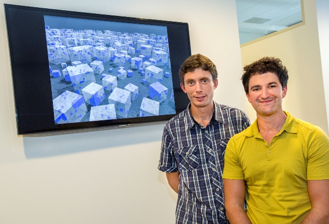
Stephen Whitelam (left) and Jeffrey Urban at Berkeley Lab’s Molecular Foundry led the first direct observations of metal nanocrystals undergoing phase transformations during reactions with hydrogen gas. (Photo by Roy Kaltschmidt)
Urban and Whitelam, both of whom hold appointments with Berkeley Lab’s Materials Sciences Division, are the corresponding authors of a paper describing this study in the journal Nature Materials. The paper is titled “Uncovering the intrinsic size dependence of hydriding phase transformations in nanocrystals.” Co-authors are Rizia Bardhan, Lester Hedges, Cary Pint and Ali Javey.
While it is well established that materials on the nanoscale can offer physical, chemical and mechanical properties not displayed at the microscale, knowledge as to how these properties can be altered as nanocrystals undergo phase transformations has been lacking.
“Quantitative understanding of nanocrystal phase transformations has been hindered by difficulties in directly monitoring well-characterized nanoscale systems in reactive environments,” Urban says.
Urban and his colleagues addressed this problem with a custom-built stainless steel gas-tight cell with optical windows and heating elements and connected to a high vacuum pump. They used this experimental setup to collect in situ luminescence spectra with a confocal Raman microscope as palladium nanocubes interacted with hydrogen gas. The nanocubes were synthesized by wet-chemistry and were all clear-faceted single-crystalline objects with a narrow range in size distribution.
“Our experimental setup allowed for rapid, direct monitoring of minuscule alterations in luminescence during hydrogen sorption,” Urban says. “This allowed us to uncover the size-dependence of the intrinsic thermodynamics and kinetics of hydriding and dehydriding phase transformations. We observed a dramatic decrease in luminescence as the palladium nanocubes formed hydrides. This lost luminescence was regained during dehydriding.”
This scanning electron micrograph shows palladium nanocubes with a side length of approximately 32 nanometers.
A statistical mechanical model whose development was led by Whitelam and co-author Hedges was then used to quantify the observational data for palladium nanocubes of all sizes. Because of the narrow size distribution of the nanocubes, Whitelam, Urban and their colleagues were able to show a direct correlation between luminescence and phase transitions that can be applied to other metal nanocrystal systems as well.
“Simple geometric arguments tell us that under certain conditions, thermally driven solid-state phase transformations are governed by nanocrystal dimensions,” Whitelam says. “These arguments further suggest ways of optimizing hydrogen storage kinetics in a variety of metal nanocrystal systems.”
The next step in this research will be to examine the effects of dopants on phase transformations in metal nanosystems.
“Our luminescence-probe and statistical mechanical model are a versatile combination,” Urban says, “that allow us to look at a number of gas-nanocrystal interactions in which controlling the thermodynamics of the interactions is paramount.”
This research was supported by DOE’s Office of Science through the Molecular Foundry and through the Center for Nanoscale Control of Geologic Carbon Dioxide, a DOE Energy Frontier Research Center. Additional support was provided by DOE’s Office of Energy Efficiency and Renewable Energy and by Mohr Davidow Ventures, a venture capital firm.
#  #  #
Lawrence Berkeley National Laboratory addresses the world’s most urgent scientific challenges by advancing sustainable energy, protecting human health, creating new materials, and revealing the origin and fate of the universe. Founded in 1931, Berkeley Lab’s scientific expertise has been recognized with 13 Nobel prizes. The University of California manages Berkeley Lab for the U.S. Department of Energy’s Office of Science. For more, visit www.lbl.gov.
The Molecular Foundry is one of five DOE Nanoscale Science Research Centers (NSRCs), national user facilities for interdisciplinary research at the nanoscale, supported by the DOE Office of Science.  Together the NSRCs comprise a suite of complementary facilities that provide researchers with state-of-the-art capabilities to fabricate, process, characterize and model nanoscale materials, and constitute the largest infrastructure investment of the National Nanotechnology Initiative.  The NSRCs are located at DOE’s Argonne, Brookhaven, Lawrence Berkeley, Oak Ridge and Sandia and Los Alamos National Laboratories.  For more information about the DOE NSRCs, please visit http://science.energy.gov.
The DOE Office of Science is the single largest supporter of basic research in the physical sciences in the United States and is working to address some of the most pressing challenges of our time. For more information, please visit science.energy.gov.

Thursday, May 30, 2013

Atom by Atom, Bond by Bond, a Chemical Reaction Caught in the Act

News Release:


Berkeley Lab scientists make the first-ever high-resolution images of a molecule as it breaks and reforms chemical bonds

MAY 30, 2013
Paul Preuss 510-486-6249  paul_preuss@lbl.gov
 84 


News Release
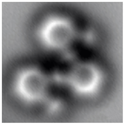
Almost as clearly as a textbook diagram, this image made by a noncontact atomic force microscope reveals individual atoms and bonds, in a molecule having 26 carbon atoms and 14 hydrogen atoms structured as three connected benzene rings.
Almost as clearly as a textbook diagram, this image made by a noncontact atomic force microscope reveals the positions of individual atoms and bonds, in a molecule having 26 carbon atoms and 14 hydrogen atoms structured as three connected benzene rings.
When Felix Fischer of the U.S. Department of Energy’s Lawrence Berkeley National Laboratory (Berkeley Lab) set out to develop nanostructures made of graphene using a new, controlled approach to chemical reactions, the first result was a surprise: spectacular images of individual carbon atoms and the bonds between them.
“We weren’t thinking about making beautiful images; the reactions themselves were the goal,” says Fischer, a staff scientist in Berkeley Lab’s Materials Sciences Division (MSD) and a professor of chemistry at the University of California, Berkeley. “But to really see what was happening at the single-atom level we had to use a uniquely sensitive atomic force microscope in Michael Crommie’s laboratory.” Crommie is an MSD scientist and a professor of physics at UC Berkeley.
What the microscope showed the researchers, says Fischer, “was amazing.” The specific outcomes of the reaction were themselves unexpected, but the visual evidence was even more so. “Nobody has ever taken direct, single-bond-resolved images of individual molecules, right before and immediately after a complex organic reaction,” Fischer says.
The researchers report their results online in the May 30, 2013 edition of Science Express.
Graphene nanostructures from the bottom up
Graphene nanostructures can form the transistors, logic gates, and other elements of exquisitely tiny electronic devices, but to become practical they will have to be mass produced with atomic precision. Hit-or-miss, top-down techniques, such as exfoliating graphite or unzipping carbon nanotubes, can’t do the job.
Fischer and his colleagues set out to engineer graphene nanostructures from the bottom up, by converting linear chains of carbon atoms into extended hexagonal sheets (polyaromatic hydrocarbons), using a reaction originally discovered by UC Berkeley professor Robert Bergman. The first requirement was to perform the reactions under controlled conditions.
“In solution, more than a dozen compounds could be the products of the reaction we were using, and characterizing the results would be difficult,” Fischer says. “Instead of a 3D solution we created a 2D system. We put our starting molecule” – a structure called oligo-enediyne, composed of three benzene rings linked by carbon atoms – “on a silver surface, and then induced reactions by heating it.”
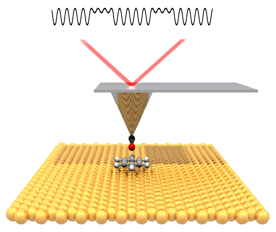
The single-atom tip of the noncontact atomic force microscope “feels” changes in the strength of electronic forces as it moves across the surface at a constant height. Resulting movements of the stylus are detected by a laser beam to compute images.
Fischer’s group collaborated with microscopy expert Crommie to devise the best possible view. The first attempt to track the reactions used a scanning tunneling microscope (STM), which senses electronic states when brought within a few billionths of a meter (nanometers) of the surface of the sample. But the image resolution of the tiny molecule and its products – each only about one nanometer across – wasn’t good enough to reliably identify the molecular structures.
The collaborators then turned to a technique called noncontact atomic force microscopy (nc-AFM), which probes the surface with a sharp tip. The tip is mechanically deflected by electronic forces very close to the sample, moving like a phonograph needle in a groove.
“A carbon monoxide molecule adsorbed onto the tip of the AFM ‘needle’ leaves a single oxygen atom as the probe,” Fischer explains. “Moving this ‘atomic finger’ back and forth over the silver surface is like reading Braille, as if we were feeling the small atomic-scale bumps made by the atoms.” Fischer notes that high-resolution AFM imaging was first performed by Gerhard Meyer’s group at IBM Zurich, “but here we are using it to understand the results of a fundamental chemical reaction.”
The single-atom moving finger of the nc-AFM could feel not only the individual atoms but the forces representing the bonds formed by the electrons shared between them. The resulting images bore a startling resemblance to diagrams from a textbook or on the blackboard, used to teach chemistry, except here no imagination is required.
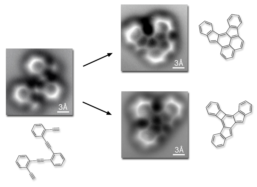
The original “reactant” molecule, resting on a flat silver surface, is imaged both before and after the reaction, which occurs when the temperature exceeds 90 degrees Celsius. The two most common final products of the reaction are shown. The three-angstrom scale bars (an angstrom is a ten-billionth of a meter) show that both reactant and products are about a billionth of a meter across.
The original reactant molecule, resting on a flat silver surface, is imaged both before and after the reaction, which occurs when the temperature exceeds 90 degrees Celsius. The two most common final products of the reaction are shown. The three-angstrom scale bars (an angstrom is a ten-billionth of a meter) indicate that both reactant and products are about a billionth of a meter across.
Says Fischer, “What you see is what you have – the effects of the electron forces among the atoms, and even the bond order. You can distinguish single, double, and triple bonds.”
A chemical bond is not as simple a concept as it may appear, however. From the dozens of possibilities, the starting molecule’s reaction did not yield what had intuitively seemed to Fischer and his colleagues the most likely products. Instead, the reaction produced two different molecules. The flat silver surface had rendered the reaction visible but also shaped it in unexpected ways.
The nc-AFM microscopy provided striking visual confirmation of the mechanisms that underlie these synthetic organic chemical reactions, and the unexpected results reinforced the promise of this powerful new method for building advanced nanoscale electronic devices from the bottom up.
Before much more complex graphitic nanostructures can result from this unique approach, says Fischer, “Large discoveries lie ahead.”
This work was supported by the Office of Naval Research, the U.S. Department of Energy’s Office of Science, the National Science Foundation, and the European Research Council.
###
“Direct Imaging of Covalent Bond Structure in Single-Molecule Chemical Reactions,” by Dimas G. de Oteyza, Patrick Gorman, Yen-Chia Chen, Sebastian Wickenburg, Alexander Riss, Duncan J. Mowbray, Grisha Etkin, Zahra Pedramrazi, Hsin-Zon Tsai, Angel Rubio, Michael F. Crommie, and Felix R. Fischer, will appear in Science and is now available on Science Express,http://www.sciencemag.org/content/early/2013/05/29/science.1238187.abstract.
For more information see the UC Berkeley release athttp://newscenter.berkeley.edu/2013/05/30/scientists-capture-first-images-of-molecules-before-and-after-reaction.
Lawrence Berkeley National Laboratory addresses the world’s most urgent scientific challenges by advancing sustainable energy, protecting human health, creating new materials, and revealing the origin and fate of the universe. Founded in 1931, Berkeley Lab’s scientific expertise has been recognized with 13 Nobel prizes. The University of California manages Berkeley Lab for the U.S. Department of Energy’s Office of Science. For more, visit http://www.lbl.gov.
DOE’s Office of Science is the single largest supporter of basic research in the physical sciences in the United States, and is working to address some of the most pressing challenges of our time. For more information, please visit the Office of Science website atscience.energy.gov.